Printed circuit board
– this is a dielectric base, on the surface and in the volume of which conductive paths are applied in accordance with the electrical circuit. The printed circuit board is intended for mechanical fastening and electrical connection between the leads of electronic and electrical products installed on it by soldering.
The operations of cutting out a workpiece from fiberglass, drilling holes and etching a printed circuit board to obtain current-carrying tracks, regardless of the method of applying the pattern to the printed circuit board, are performed using the same technology.
What is a printed circuit board?
A printed circuit board (PCB) is used to mechanically assemble radio components and connect them electrically using conductive patterns, pads and other components etched onto the copper layer of the laminated wafer. The PCB contains pre-designed copper tracks. Properly designing connections through these traces reduces the amount of wire used and therefore the amount of damage caused by broken connections. The components are mounted on the PCB by soldering.
Drilling holes
It is best to drill holes using a special mini drilling machine with a carbide drill with a diameter of 0.7-0.8 mm. If a mini drilling machine is not available, then you can drill holes with a low-power drill using a simple drill. But when working with a universal hand drill, the number of broken drills will depend on the hardness of your hand. You definitely won’t be able to get by with just one drill.
If you cannot clamp the drill, you can wrap its shank with several layers of paper or one layer of sandpaper. You can wrap a thin metal wire tightly around the shank, turn to turn.
After finishing drilling, check whether all holes are drilled. This can be clearly seen if you look at the printed circuit board up to the light. As you can see, there are no missing holes.
Applying a topographic drawing
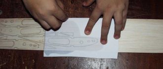
In order to protect the places of foil on fiberglass laminate that will be conductive paths from destruction during etching, they must be covered with a mask that is resistant to dissolution in an aqueous solution. For the convenience of drawing paths, it is better to pre-mark them using a soft pencil or marker.
Before applying the markings, it is necessary to remove traces of the glue that was used to glue the printed circuit board template. Since the glue has not hardened much, it can be easily removed by rolling it with your finger. The surface of the foil must also be degreased using a rag using any means, such as acetone or white alcohol (the so-called purified gasoline), or any dishwashing detergent, for example Ferry.
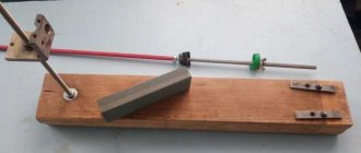
After marking the tracks of the printed circuit board, you can begin to apply their design. Any waterproof enamel is well suited for drawing paths, for example alkyd enamel of the PF series, diluted to a suitable consistency with a white alcohol solvent. You can draw paths with different tools - a glass or metal drawing pen, a medical needle, and even a toothpick. In this article I will tell you how to draw circuit board traces using a drawing pen and ballerina, which are designed for drawing on paper with ink.
Previously, there were no computers and all drawings were drawn with simple pencils on whatman paper and then transferred in ink to tracing paper, from which copies were made using copiers.
Drawing begins with contact pads, which are drawn with a ballerina. To do this, you need to adjust the gap of the sliding jaws of the ballerina drawing board to the required line width and to set the diameter of the circle, perform the adjustment with the second screw, moving the drawing blade away from the axis of rotation.
Next, the ballerina's drawing board is filled with paint to a length of 5-10 mm using a brush. For applying a protective layer to a printed circuit board, PF or GF paint is best suited, since it dries slowly and allows you to work quietly. NTs brand paint can also be used, but it is difficult to work with because it dries quickly. The paint should adhere well and not spread. Before painting, the paint must be diluted to a liquid consistency, adding a suitable solvent to it little by little with vigorous stirring and trying to paint on scraps of fiberglass. To work with paint, it is most convenient to pour it into a bottle of manicure varnish, in the twist of which there is a solvent-resistant brush installed.
After adjusting the ballerina's drawing board and obtaining the required line parameters, you can begin to apply the contact pads. To do this, the sharp part of the axis is inserted into the hole and the base of the ballerina is rotated in a circle.
With the correct setting of the drawing pen and the desired consistency of paint around the holes on the printed circuit board, perfectly round circles are obtained. When a ballerina begins to paint poorly, the remaining dried paint is removed from the gap of the drawing board with a cloth and the drawing board is filled with fresh paint. To draw all the holes on this printed circuit board with circles it took only two refills of the drawing pen and no more than two minutes of time.
Once the round pads on the board are drawn, you can start drawing the conductive paths using a hand drawing pen. Preparing and adjusting a manual drawing board is no different from preparing a ballerina.
The only thing additionally needed is a flat ruler, with pieces of rubber 2.5-3 mm thick glued to one of its sides along the edges, so that the ruler does not slip during operation and the fiberglass, without touching the ruler, can freely pass under it. A wooden triangle is best suited as a ruler; it is stable and at the same time can serve as a hand support when drawing a printed circuit board.
To prevent the printed circuit board from slipping when drawing tracks, it is advisable to place it on a sheet of sandpaper, which consists of two sandpaper sheets sealed together with the paper sides.
If they come into contact when drawing paths and circles, then you should not take any measures. You need to let the paint on the printed circuit board dry until it does not stain when touched, and use the tip of a knife to remove the excess part of the design. In order for the paint to dry faster, the board should be placed in a warm place, for example, on a radiator in winter. In the summer - under the rays of the sun.
When the design on the printed circuit board is completely applied and all defects are corrected, you can proceed to etching it.
Another way to apply a design to paper using a laser printer.
Making printed material using a laser printer and an iron is a rather tedious process, but it gives a pretty good result if you practice a little.
1 . Carefully glue a sheet of fax paper (glossy side up) onto a sheet of regular paper (to compensate for the lack of faxing rigidity). For what? It is necessary to first run the paper through the printer/laser oven for shrinkage. To smoothly pull through the tract, simply iron the thermal paper on the sensitive side with an iron. 2 . Paper - take the base from self-adhesive paper, or thermal paper for faxing, definitely thermal paper, and prepared - first iron the sheets with a hot iron until flat (at the same time they will turn dark brown, then bluish-gray), fold them in this form for future use. Before outputting the board, run the sheet through the printer - for example, by printing a blank page. The minimum sheet size is ~6*12 cm for HP 5/6L. 3 . Print at maximum boldness, mirror image. printing and transferring to the blank can be up to a week apart, I haven’t tried it again (this is for those who don’t have a laser at home). 4 . Take the workpiece with a margin of 3-5 mm on each side. foil - lightly sand with zero polish and wipe. There should not be any harmful deposits such as white sediment from denatured alcohol. I use isopropyl alcohol or “galosh” (aka “lighter”) gasoline. 5 . Iron - with a normal, smooth surface. reheat in advance. Temperature - for waxing you need to select it more carefully (I have a display meter set to “artificial silk”), otherwise the impregnation will begin to transfer. for thermal paper - higher is possible. 6 . There should be no dust or any small things, neither on the foil nor on the paper. 7 . Make a sandwich - on a flat thick plywood (although I have 3mm paper), put a piece of thick cardboard, a blank board, blow off the dust, drawing, for thermal paper (it's thin) - also a piece of moderately thick paper, a hot iron. 8 . You begin to move with the iron, pressing with a force of ~5..10 kg/sq.dm. wait about two minutes for it to stick. 9 . Tilting the iron very slightly, you roll out individual tracks for a couple of minutes. It is very important here not to crush the tracks, and at the same time to weld them. From time to time you need to lower the iron to the entire plane so that the rest of the iron does not cool down. The thermal paper clearly shows the difference in welded and defective pieces. 10 . Well, you iron for another minute to clear your conscience and put the iron away. The sandwich cools and sections of paper between the tracks swell. We don’t wait for it to cool down, put the board directly under a stream of boiling water. eleven . Now the board - under running water and a piece of wet foam rubber, you begin to erase the paper. You cannot tear it off in large pieces or from dry foil. You need to remove clumps of paper from the foam rubber more often. We take the paper by the corner and tear it off. Then we remove the remains with our finger/rag/foam rubber. 12 . Use a new piece of sponge to wipe off the lint (as much as possible), and look at the wet pattern under a magnifying glass. if there are many defects, or they are located in inconvenient places - see point 1, with variations in parameters. 13 . Cover the reverse side with strips of wide tape and etch. It is possible even in boiling FeCl3
Drawing.
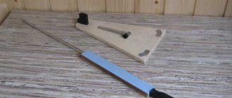
In our circles, of course, we argued a lot about the paint used and the technology for applying the paths, but I settled on what is described below. Drawing is done with nitro paint, with rosin powder dissolved in it (provides plasticity for correction for some time after drying and does not allow the paint to “lag behind” in the case of etching with hot solutions). Drawing is done with glass drawing pens (which are very difficult to find these days). In addition, it is possible to use as a paint, asphalt-bitumen varnish, dissolved to the desired condition with xylene. The bottle will last a very long time. It is possible to make drawing feeders yourself, with appropriate training, of course. To do this, you can take a thin-walled glass tube and stretch it over a flame (over a gas stove) and break it in the middle. Then “finish” the broken tip on fine sandpaper. Next, after heating over the same flame, bend the tip to the desired angle. Difficult!? In fact, no more than 5 minutes. You can also use disposable syringes for drawing. The varnish is drawn into a disposable syringe (1-2 ml) and a thin needle is inserted. Before installation, the needle must be processed with a file so that the edges are smooth (remove the sharp end). From the side of the piston, you can insert another needle to allow air to pass inside the syringe.
Before you start drawing the printed circuit tracks, you need to draw the mounting pads for soldering the elements. They are applied using a glass pen or a sharpened match around each hole, approximately 3 mm in diameter. Next you need to let them dry. After this, you need to cut them using a compass to the required diameter (I use a small compass-measuring device with a threaded distance lock (may professional draftsmen forgive me for this expression, I never knew its real name), one of the needles of which is ground into a flat cutter). Next, the trimmed excess is cleaned with an awl or scalpel. In fact, I use a recycled school utensil for these procedures. The result is smooth round areas of the same diameter, which can only be connected by tracks, according to the previously drawn drawing of the printed circuit board. Next, after drying, the second side is drawn. Then the tracks and errors are corrected using a scalpel. Moreover, it should be noted that in order to align the edge of the track, you must first trim the edge using a ruler (preferably a metal one), and then remove the excess by scratching. If you clean the path right away, then, depending on the degree of dryness of the paint, you can get “chips” even worse than the original ones. Check that the pattern on the board matches the pattern on the drawing.
Method of applying a design to a paper using a laser printer
I do everything much simpler: I take a blank and a simple Soviet eraser. I thoroughly wipe the entire board with an eraser. All oxidation is removed. Just in case, you can wipe it with gasoline (but I don’t do this, an eraser is enough). Then I take the thermal paper from the fax machine and iron it with an iron. It turns gray-violet. I insert this paper into the printer (I have an HP 6L and I don’t glue any paper for rigidity, I haven’t chewed it yet) and mirror print the board design. I put the paper on the paper and start fiddling with the iron. My power is at 3/4 of the maximum power. I iron for 3-4 minutes. Then I throw the workpiece into hot, warm water and wait 5 minutes for the paper to soften. Then I use a sponge or fingers to roll the paper off the board. Do not pick up the edge of the paper or tear it off; the tracks may come off along with the paper! Just roll it off the board. Next I core, drill, trim and etch. And the board is ready.
The practice of printing on foil PCB
There are two options: order the production of a printed circuit board in a service or make a printed circuit board with your own hands directly at home. The first option requires a substantial financial investment and two to three weeks of waiting. The second does not require anything other than personal desire, a piece of foil PCB and a small amount of ferric chloride.
PCB sheets, laminated on one or both sides with a thin layer of copper, are traditionally used for the manufacture of printed circuit boards. Typically, a rigid base with wiring of electronic circuits for soldering electronic parts is a priority for the specialized production sector. However, designing electronics for personal needs and in small copies looks more rational when the technology for producing “signatures” is available in everyday conditions.
It is quite possible to obtain such a result of work at home, using simple accessible means, tools, materials
If you master all the intricacies of production and stock up on the necessary materials, it is not impossible to manufacture printed circuit boards at home, if not on an industrial scale, then in quantities sufficient for business. There are several technologies for drawing and etching miniature tracks on foil PCB.
Starting from the method of simply drawing an electronic circuit with nail polish followed by chemical etching, and ending with automatic laser layout and micron cutting. However, for home conditions, a special technique is required - effective, but at the same time inexpensive and relatively uncomplicated.
Errors during production
Common mistakes include overheating the board and poor etching solution. Always mix all the components of the solution, otherwise it will not begin to etch the board. Soldering acid should not be used when tinning the board. It will damage the board over time if you don't clean it well.
Some radio amateurs also have the practice of tinning boards with Rose alloy. You should not do this, since such an alloy is intended for desoldering parts, and not for permanent soldering. In addition, it is fragile and will quickly oxidize over time.
