Soldering printed circuit boards is a procedure for electrically and mechanically connecting electronic components on a dielectric plate using molten metal - solder. This technique is also called surface mounting technology (SMT) or SMT (Surface Mount Technology).
Installation of printed circuit boards is a rather labor-intensive process used in the production of radio-electronic components. It first appeared in the 60s. XX century, and became widespread in the field of radio electronics in the late 80s. The main difference between this method and the “traditional” ones is manifested in the use of solder (or solder paste) pre-applied to the plate, followed by tinning, as a result of which the connection becomes stronger and more reliable.
Wave method
In the process of mass production of electronic devices, components are mounted on printed circuit boards on factory conveyor lines. In this case, wave soldering is used.
The essence of this technology, which appeared in the 50s of the last century, is as follows.
Printed circuit boards with electronic components installed on them move along a special conveyor. During the movement, the soldering areas are covered with flux, the board is preheated, and then passes over a bath of molten solder.
The bath is equipped with special nozzles that create a wave rising above the surface of the solder in the bath.
The board is positioned in such a way that the soldering points are in contact with the surface of the wave as the board moves along the bath. At this moment, the contact pads on the board and the leads of the soldered parts are wetted with solder.
The surface tension of liquid solder prevents it from completely draining from the surface of the board, which ensures soldering of parts to contact pads.
Setting process parameters
To obtain high-quality solder joints, it is necessary to adjust the technological parameters of the soldering line. Firstly, the shape and orientation of the nozzle forms a wave crest with an optimal profile, and secondly, the board moving above the bath is located at a certain angle to the surface of the melt.
Correctly selected process parameters make it possible to avoid defects in the form of jumpers between current-carrying tracks and sagging (icicles) on the terminals of parts.
Double wave soldering technology can be used for the same purpose. In this case, the first wave of solder is turbulent in nature, which allows better wetting of the soldered surface and penetration of solder into the mounting holes of the board.
The second wave, which has a smoother laminar flow, washes away flaws in the form of excess drops and sagging of solder, while forming the final geometry of the dumbbells.
Wave soldering is not always automated. For example, on many assembly lines in China and other Asian countries, people install parts on the board, then apply flux and dip the board into a solder bath.
In this case, the board is taken by hand using a special grip and dipped into a bath of liquid solder.
Mounting SMD components
The wave soldering method is most often used for boards whose components are mounted on one side of the board, and pads and current-carrying tracks on the other.
The pin terminals of the elements are inserted into the through holes of the board and soldered on its reverse side. However, most modern electronic circuits are designed using so-called SMD components, secured by surface soldering. Such parts are soldered to the board on the same side on which they are installed.
The use of wave soldering technology for such elements has a number of features:
- when wave soldering SMD components, the board should be oriented downward with parts previously glued to it;
- a wave of molten solder washes over the body of the parts.
Thus, SMD components must be glued to the board with special glue before soldering. At the same time, sometimes there are cases of parts peeling off during their contact with the melt wave, which leads to the appearance of defects.
In addition, not all electronic components are able to withstand the temperature conditions that arise during the process of “bathing” in liquid solder. These circumstances limit the use of wave technology.
We should add one more negative feature inherent in this soldering technology. A large amount of molten solder in the bath, constantly in contact with open air, leads to the active formation of oxide.
Restoring tracks on a laptop motherboard
Let's get acquainted with an unusual renovation.
We have a laptop. Complaints about the laptop are that when you touch the laptop, it can turn off spontaneously; the battery is not charging; Didn't always respond to the power button.
In one of the service centers, the contact pads under the BIOS chip were damaged in a laptop while trying to flash it.
For clarity, let's look at the image.
This image shows that the textolite, under which there were contact pads, was simply scratched to the inner layer. The paths are torn off. They tried to solder them.
We carry out repairs in the following way.
First, the contact pads that were scratched were covered with tsapon varnish. We waited for the varnish to dry.
Then all the traces that went to the pads were located and checked to ensure they were soldered correctly.
Then, after first comparing with the circuit, we laid new paths of wire hairs to the contact pads.
Since one contact pad under the microcircuit was alive, we soldered to it first.
Then we fixed the chip in the lower right corner, as seen in the image above. And only then were all the tracks unsoldered.
Let's take a look at the next photo.
Here the microcircuit is already secured with a small amount of glue on the sides so that during further operation the microcircuit is not damaged.
We used a special glue that melts when heated and can be easily removed if necessary.
The microcircuit now looks like this in real life.
The microcircuit is not in the best location. The lid is just pressed there. Therefore, the soldering must be of very high quality so that the microcircuit does not come off under mechanical stress.
Checking the laptop for functionality after repair was successful. The laptop started up normally. The battery immediately caught the charger and began charging.
Let's open the "CPU HWMonitor" program. This useful program shows the temperature that is in the system - the temperature of the motherboard, processor, graphics, etc.
So, if, for example, the processor temperature is too high relative to the recommended one, this is a reason to check the thermal paste.
Here you can find out the parameters of the laptop battery - its voltage, capacity and percentage of battery charge.
If all the parameters are satisfactory, the laptop works without failures, then it can be assembled normally and used fully.
Link to video instructions:
- < Back
- Forward >
Solder Paste Application
To attach SMD components to the board, other soldering technologies are usually used. As a rule, they are all based on the use of solder paste. This composition includes powdered solder, flux and filler.
Solder paste is applied to the contact pads of the board and the leads of the parts installed on them.
After this, the board is sent to a special oven, where the connections are heated in one of the following ways:
- steam-gas mixture;
- sources of infrared radiation;
- by convection method.
During the heating process, the solder paste melts and the contacts are soldered.
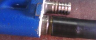
Loop extension
In the case where a break is detected between the moving parts (at the place of permanent bending of the cable), it will need to be extended.
To do this, you can use an insert with a similar structure, the width, number of tracks and their size correspond to the ribbon being restored.
At the beginning of the repair, you should cut the cable at the point of damage and clean each track on both sides. The same will need to be done with the previously prepared insert.
The main thing is to carefully ensure that the tracks on all connected sections of the cable are accurately aligned.
After this, all that remains is to solder each of the connected parts, just as it was done for the two ends.
After connecting the contacts, remove excess flux with a solvent and check the quality of soldering using a magnifying glass. After this, it is necessary to further isolate the restored areas using adhesive tape.
Automated technologies
In situations where electronic components have pins with very fine pitches, when soldering connectors with a large number of pins, and in other cases that require the use of very fine technology, a soldering robot is usually used.
A robotic manipulator for soldering boards is a precision device containing a coordinate table on which a board with parts placed on it is installed and a soldering head moving along three coordinate axes.
The head is equipped with a solder supply mechanism and a device for vacuum suction of excess solder.
Robotic automatic soldering of circuit boards is significantly inferior to the wave method in terms of speed, so it is used only in cases where the latter cannot be used.
In addition to the actual soldering, robots are often used to install parts on the board immediately before soldering them. Individual elements, the installation of which due to their complex non-standard shape (transformers, chokes, some types of microcircuits) are difficult to automate, are installed manually.
Therefore, even on large assembly lines of well-known companies that produce electronic equipment, there are areas where assembly is carried out by people.
In addition, product quality control is also often performed by humans. Boards with defects that can be eliminated are sent for modification, which is done manually with a soldering iron.
Working at home
When assembling homemade electronic devices, radio amateurs make their own printed circuit boards. If you have the desire and basic training, this is not difficult to learn.
You can make a printed circuit board using the existing drawings of the tracks on the board; those who are more prepared can independently make a sketch of the board, having a circuit diagram of the device. To make a printed circuit board, a sheet of foil insulating material is taken.
This can be getinax or fiberglass, coated with a thin layer of copper on one or both sides, depending on what type of board is required - single-sided or double-sided.
A sketch of the pattern of current-carrying paths is drawn on paper, then it is transferred to the surface of the copper layer, through holes are drilled in the right places to install parts, and the pattern is covered with a layer of paint or varnish.
After the coating has dried, the board is etched, that is, it is immersed for some time in one of the compounds that corrodes the layer of copper that is not covered with paint. Usually, for these purposes, either ferric chloride, an acid solution, or a mixture of copper sulfate and table salt is used.
After etching the copper, the varnish or paint is washed off with a solvent, the resulting pattern is tinned with a regular soldering iron, after which you can begin installing the parts and soldering them to the board.
Before tinning, the tracks should be thoroughly degreased and cleaned with fine sandpaper. The leads of the parts also need to be cleaned before installation; you can also tin them, this will make the subsequent soldering process easier.
Soldering is done with a well-heated soldering iron, on the tip of which there should be a drop of solder. If the solder melted by a soldering iron does not stay on the tip, the soldering iron is most likely overheated.
To control its temperature, it is better to use a voltage regulator or soldering station. Contact between the soldering iron and the part should be short. After wetting the pin of the part and the pad on the board with solder, the soldering iron is immediately removed.
Read also: Paint with acrylic paint using a spray gun
This will eliminate the possibility of the part failing as a result of overheating and will ensure an even and beautiful spreading of the solder drop.
For soldering circuit boards and electronic components, you should choose soft grades of tin-based solders. In this case, the required soldering strength will be provided by the softest solder, while its use will facilitate the work and reduce the thermal load on the parts.
Since the terminals of electronic components are usually already tinned, and the board tracks are made of copper, only rosin or its alcohol solution can be used as a flux.
The ability to solder boards can also be useful when performing independent repairs of failed electronics.
How to solder a resistor to an LED
If your circuit does not provide for current limitation by the so-called driver, then you can use resistors the old fashioned way.
It is impossible to connect LEDs directly to the network, since in addition to the increased current, it is also variable. The resistor and driver convert the current to direct current.
Each LED ideally needs a separate resistor. This is if there are few diodes. If there are, for example, a hundred of them, as in some garlands, or even a couple of dozen, you will have to purchase a driver.
If you are encountering the concepts of “resistor” and “driver” for the first time, we have selected visual instructions:
The resistor must be connected in the circuit after the power supply and before the LED. It just solders. In the chapter “Features of soldering” we left a video on how to solder any contact (see above). There are no special features here. The only thing that can be doubted is the choice of flux, that is, a substance that cleans the contact surface from oxide and/or grease film. As an option - a special paste.
Installation and Soldering Basics
The tools and materials necessary for the work are discussed in lesson No. 1. Let me briefly remind you of what is needed to assemble the constructor: a soldering iron, solder with a rosin channel, radio side cutters, tweezers, a third-hand type board holder, alcohol, napkins, an old toothbrush, a table, a table lamp, a chair. So, let's start assembling. We will be assembling the Master Kit NS073 - “Living Heart”, although for training purposes it is completely unimportant which kit we consider assembling. This is what you should end up with:
The LEDs of the assembled device blink effectively, creating a very beautiful “running fire” effect. But first you need to assemble the set. To do this, you will need to install each part in its place, and then solder all the parts. You never know what you can do till you try. Let's get started!
General requirements for the workplace. Security basics
Even though we already talked about this in Lesson No. 1, it’s worth mentioning these serious things regarding security again:
– the workplace (table) should not be cluttered. It is more pleasant and efficient to work on a free desk. In addition, radio components will not be easily lost in the surrounding trash; – Since the radio components are small, the workplace should be well lit to avoid unnecessary eye strain. Always turn on the desk lamp; – during soldering, ensure good ventilation of the workplace. Open the window, or turn on the table fan, which drives the smoke away from the soldering iron; – the soldering iron is hot! Just hold on to his handle. Do not allow your fingers to touch the sting; – after soldering, as after any other work, always wash your hands.
Printed circuit board
The printed circuit board is the main one, the chassis is the whole structure. All parts are installed on the front side of the board (the one where there are inscriptions), and the pins of the parts are soldered on the back side (where there are conductive tracks).
Installation of resistors
Let's say we want to install resistor R1. Using the table from the instructions, we determine that R1 should have a resistance of 1 MOhm. We find a resistor of the appropriate value in the set (how to determine the value of the resistor is described in lesson No. 2). We are looking for mounting location R1 on the printed circuit board. In order for resistor R1 to “fit” comfortably into its intended place on the printed circuit board, the resistor leads need to be molded, that is, bent in a certain way. You can bend the leads with your fingers or using tweezers. If you didn’t manage to bend the leads correctly the first time, it’s okay, you can correct the molding. But we must remember that if you bend the lead in one place more than several times, it may break off.
This is what the installed resistor looks like from different angles:
Resistor R1 is installed “vertically”, that is, its body is located above the surface of the board. The angle between the component and the housing can be any, this does not affect the quality of the circuit. Also remember from lesson No. 2 that the resistor has no polarity, that is, it can be installed either with the brown stripe up (as in the figure) or with the brown stripe down.
To prevent the part from falling out when turning the board, bend the resistor leads on the back side of the board in different directions:
We can immediately trim off the excess resistor lead and solder it. Then install the next part, cut its leads again and solder... But you can first install all the parts, then cut their leads, and then solder them all at once. This will turn out faster, more technologically advanced, this is exactly what professional installers do in production. We will also act this way.
Let's install resistor R2. Please note that this resistor is installed “horizontally”, that is, its body is closely adjacent to the plane of the printed circuit board. Accordingly, the shape of the terminals of this resistor is somewhat different.
Let me remind you again that resistors have no polarity. In this case, the blue resistor strip is on the right. But you can also install it in the opposite direction - with a blue stripe to the left. In the same way we install all the other resistors (there are 9 of them in this set).
Installation of capacitors
There is only one capacitor in this set - C1, so it is impossible to confuse it with any other. But still, let’s check that the capacitor code 104 is indicated on the capacitor in full accordance with the list of components. In this case, the capacitor leads do not need to be molded, since the component is perfectly installed on the board in the factory state of the leads. We also know from lesson No. 2 that a ceramic capacitor has no polarity and can be installed on the board in any position. If some other set contains several ceramic capacitors, you need to use the capacitance code indicated on the component to determine which seat it should be installed on - C1, C4 or C17, for example. There are no other capacitors in the NS073 kit, but for training purposes, using the example of another kit, we will also consider installing an electrolytic capacitor. We remember that the electrolytic capacitor must be installed taking into account its polarity.
Diode installation
We find the seat for diode VD1 on the printed circuit board. Let's remember from lesson No. 2 that a diode has polarity. Please note that on the printed circuit board there is a diode “key” designation - a stripe near one of the terminals. The same stripe is present on the diode itself. When installing the diode, you must strictly adhere to the polarity marks. If you install the diode in the wrong polarity (in this case, the wrong installation is with the strip facing up), then the circuit will not work. Moreover, the diode or other circuit elements may fail in this case.
The forming of the diode leads is similar to that of resistor R2.
Transistor installation
There are no transistors in the NS073 set, but for the sake of completeness, we will consider installing a transistor using the example of another set. Remember that the transistor has a “key”, which during installation must be aligned with the corresponding mark on the printed circuit board.
In addition, it is important to remember that different transistors may be identical in appearance. And if the set includes two or more transistors, it is necessary to check the markings on their cases and install the components strictly in the required positions - VT1, VT2, etc.
Chip installation
This set includes two microcircuits. When installing, you must follow their keys, indicated by notches both on the printed circuit board and on the component itself. We bend the pins of the microcircuit - not necessarily all of them, two opposite ones are enough. The chip is fixed and will not fall out. In addition, we must take into account that the DD1 and DD2 microcircuits are different. True, in this case the microcircuits have a different number of pins: one has 14, and the other has 16, so during installation you will immediately understand if you are doing something wrong. But it happens that different microcircuits have the same housings with the same number of pins. Therefore, always pay attention to the markings on the microcircuit housings and the information in the instruction plate listing the components.
Read also: DIY tool rack
Jumper installation
Some kits, and NS073 in particular, require a step such as installing a jumper. A jumper on a printed circuit board is indicated by a line:
The jumper is not an electronic component and is not included in the kit. It can be done either from a small piece of wire or from cutting one of the terminals of any radio component. A jumper is formed in the same way as a resistor.
LED installation
An LED is a type of diode. And it also has polarity, which is important to observe during installation.
The “+” (anode) terminal of the LED is indicated on the printed circuit board.
The LED itself has a longer “+” (anode) terminal. But you can only focus on this key before cutting the diode leads. There is another polarity mark - a bevel on the diode body at the cathode terminal (“-”). We mount all the LEDs (there are 20 of them in the NS073 set). We bend their leads to the back of the board. There are a lot of protruding pins, the board takes on a sloppy appearance, but there is no need to be afraid of this, at the next stage we will trim off the extra pins. If the leads are very disturbing, you can cut off some of them or even all of them during the installation process. How to do this is described below.
Lead trimming
This is the “horror” we see on the back of the board after installing all the components.
Now we will bring the board into a neat appearance by cutting off the leads (or, as they say in the jargon of radio installers, we will “comb” the board).
We will need radio engineering side cutters (more details about this tool are described in lesson No. 1). We hold the tool almost perpendicular to the board. Leave about 1-2 mm from each terminal. A pin that is too long will stick out unsightly. In addition, long leads of different components can short-circuit with each other during subsequent soldering and form parasitic jumpers. A lead cut too short may cause the component to fall out. It is desirable that the lead does not extend beyond the contact pad. The pictures below show an excessively long lead and a lead of optimal length.
Thus. cut off all leads. As a result, we will get something like this:
The board is ready for soldering.
Soldering of the structure
The soldering tools required to assemble the kit are described in Lesson No. 1. Let me briefly remind you: you will need a soldering iron (or soldering station) and solder with a rosin channel. It is also convenient to use a board clamp - the so-called “third hand”.
It is convenient to fix the board using a special “third hand” type holder, or in some other way.
In one hand (for right-handers - in the right) we take a soldering iron, in the other - a solder bar. Of course, the soldering iron must be hot. It does not become this way immediately after being plugged in, but a few minutes after that. If you bring a hot tip to the solder, it will begin to melt.
Place the soldering iron tip on the soldering point. Pay attention - not to the tip of the part, but to the contact pad. At the same time, we feed a solder bar to the same point. Like the tip of a soldering iron, we feed the rod not to the tip of the lead, not to the soldering iron, but to the contact pad. The solder begins to melt. We slightly feed the rod to the soldering point, while slightly moving the soldering iron. That's it, we have formed a soldering point. Remove the solder and then the soldering iron. We wait a second - the solder has frozen, the soldering point is ready. The soldering point requires 2-3 millimeters of solder rod (this is very approximate data, depending on the type of solder and contact pad). The process goes much faster than I talk about it. It takes me about a second to complete one soldering point. Acceptable - up to three seconds. If you heat the solder point longer, problems could theoretically arise: you could overheat the part, or a pad or trace could peel off from the board base. But in practice this is unlikely. The Master Kit includes only high-quality boards, and the components in construction kits for beginners are not so “delicate” and forgive many mistakes, including overheating.
High-quality soldering is shiny and smooth. If the soldering is loose and matte, it means you are using low-quality solder (or solder without a rosin channel), or the soldering iron is either not hot enough, or, as is most often the case, too hot. I talked about soldering technology, in which a solder rod is fed directly into the soldering zone, and the tip is used only as a heater. For modern tips made of low-burning materials, this is the only correct technique. If you are using a soldering iron with a regular copper tip, you can melt some solder on the tip, and transfer the liquid solder to the soldering point on the tip, like on a shovel. Try it - maybe it will be more convenient for you. Everything is very simple. But it's like football: it takes practice. You can read many volumes on football theory, but this does not mean that you will learn to play it. Practice is something different and absolutely necessary.
Washing the board
Strictly speaking, modern fluxes included in solders allow a no-clean process. That is, you don’t have to wash the board. But such a printed circuit board looks ugly, soldering defects are poorly visible on it, and in general there is such a concept - “production culture”, and every self-respecting manufacturer of the board washes it. Special cleaning machines are used in production, but spending several thousand dollars and purchasing such a machine the size of half a room is not practical for a radio amateur. Good results can be achieved using alcohol, an old toothbrush and napkins. Wetting the brush, we thoroughly polish the board from the solder side; at the final stage, it is convenient to use napkins to clean and dry the board. Now our assembled board is clean, beautiful, and people are not ashamed to show it. After washing, it is easier to find defects on the board. Therefore, look carefully at the board again and make sure that all contact pads are well soldered and there are no parasitic short circuits. If necessary, we eliminate defects.
Elimination of soldering defects
In the figure below there are two soldering defects: one of the pins is not completely soldered, only on one side. Such contact is unreliable (in professional jargon this is called “not lost”). We simply forgot to solder the other output. A structure assembled with such soldering defects may either not work at all or be unstable.
We will correct the defects by re-soldering the identified problem soldering points.
Sometimes during the soldering process, parasitic connections are made by soldering adjacent pins:
If you do not notice such soldering defects, then the finished structure may not only fail to work, but may even fail immediately after switching on. Therefore, it is necessary to carefully check the installation. Let's say we discovered a parasitic short circuit (in radio engineering jargon, such a defect is often called the cacophonous “snot”). I'll tell you how to restore normal soldering.
Read also: Press fit designation on the drawing
1. Using a knife (scalpel). We heat the defective soldering with a soldering iron, and use a sharp blade to pass between the soldering points. The defect has been fixed. 2. Using a special tool - a vacuum pump, which is also called “radio-technical suction”. We warm up the soldering area, bring the suction device, press its button - the excess solder is drawn into the tool. Soldering fixed! 3. Using a special radio engineering “braid”. We warm up the soldering area, insert a multi-core copper “braid” into the soldering area - under the influence of tension forces, excess solder is absorbed onto the “braid”. Soldering fixed!
In the next lesson I will talk about how to configure and connect the assembled structure.
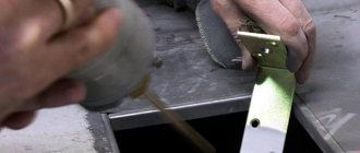
Every man should know how to use a soldering iron. Today we will talk about soldering boards. Boards are usually soldered with tin-lead solder, which melts at a temperature of 180-200° C. It is better to use low-melting Wood's composition, the melting point of which is 70° C.
A device for desoldering electrical radio elements from a printed circuit board.
Along with solder, flux is used to protect parts from oxidation during soldering. The flux used for working with circuit boards should not contain acid. The most common flux is rosin. You can grind natural pine rosin into powder and dissolve it in ethyl or boric alcohol. Liquid rosin is applied to the desired areas with a brush.
Join the discussion
You are commenting as a guest. If you have an account, log in to write on your behalf. Note: Your post will require moderator approval before it will be visible.
Related publications
Hello everyone, I have this soldering iron (attached a photo), after purchasing it I turned it on, decided to check it and tin it, the soldering iron got hot (and the tip too) to red and the tip burned out, as I understand it (the photo shows the second tip, not the original one), I changed the tip as shown in the photo, after an hour of work under load (soldering with flux, I used TAGS flux (if I understood correctly, this is glycerin flux)), the tip turned black and did not tin, I tried cleaning it with metal shavings, but to no avail. In general, as I understand it, it’s overheating, and I’m thinking of putting a diode in the gap of one of the wires, I’d like to know your opinion, is it overheating or a problem in the tip, I haven’t cleaned the tip with anything. Thanks in advance for your answers.
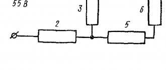
Good day, dear radio amateurs! I ask for help with the following question: I came across an N 3013 oscilloscope (circuit attached) for restoration (for myself), the former owner tried to incorrectly measure the frequency in the 220 socket and the board flew. I restored the power part, the part that controls the beams (along x and y), but the part that is responsible for amplification, synchronization, sweep (sorry if I made a mistake in the purpose of the required part of the circuit) cannot be restored. That is, as it is not subject to, it requires reassembly, but. Unfortunately, I don’t have the amplifier chip at hand. The essence of my question is whether it is possible to replace the amplifier microcircuit in the circuit with another one? There are K140UD2A and K157UD2 available. I would appreciate your advice.
Hello. I installed a board with a microprocessor and decided to use tps65261 for power supply. I took the circuit from the datasheet, removed the unnecessary stuff (VDIV to turn off the input voltage control, EN in the air for autostart, I don’t use PGOOD and RESET). I ordered the board with SMT installation, i.e. all components are placed correctly. I didn’t understand the COMP pins, I connected them approximately as in the datasheet. Upon receipt, I discovered that the GND pins were not soldered, so I first soldered the contacts with bottom heating 200* (highly heat-intensive, it would not have worked without it). When 5V power is supplied, the current consumption is 150mA, the voltage does not rise, the EN pins produce a voltage of only +-2V. I checked it with an oscilloscope, nothing else happens, SS does not rise. I have no idea where to look, since this is the first time I’m using such converters. The problem is not in a specific instance, 3 boards have the same behavior. Connection diagram:
In hardware (I didn’t notice that I moved the SMD, but it doesn’t affect the operation): C Layout in KiCad: PCB.kicad_pcb Datasheet: https://www.ti.com/lit/ds/symlink/tps65261.pdf
Hello! I'm designing a microcontroller board (STM32F405RGT6) with minimal configuration. Is this a normal circuit that I have developed? The microcontroller will be loaded with firmware via USART1. BOOT1 and BOOT0 are connected to jumpers. Please show me my design mistakes. I was guided by AN4488. The electrical circuit diagram is attached in the files below in PDF or JPEG format. Thank you!
UV LED matrix boards for exposure of photoresist and protective mask are sold. Board 100×86 - 199 rubles, 7 boards available. Delivery by Russian Post at the buyer's expense. The boards can be assembled in a field of a larger area, 12V power supply, 100 UV LEDs.
Preparation for soldering
The requirements for soldering equipment are:
Sequence of servicing parts leads.
- The best option is a soldering station. It includes everything you need (at a cost of 800 rubles).
- The power of a conventional soldering iron should not exceed 40 W.
- The supply voltage can be 12 V, 18 V, 24 V, 220 V. There are also gas tools.
- It is advisable to have several stings of different shapes and sizes in the kit.
- The heat-resistant tip is very convenient.
- The correct flux, sold in syringes, will ensure good soldering quality.
- Solder is most often used in the form of wire with a diameter of 1-5 mm. The most common diameter is 1.5-2 mm.
- You will need a knife, small wire cutters, and tweezers.
Preparing the soldering iron
A brand new soldering iron needs to be prepared for use. When turned on, oily substances usually burn and produce a sufficient amount of smoke. After burning out, the soldering iron is turned off and cooled. The soldering iron tip must be cleaned with a file. Then it is turned on again, the stripped tip is dipped in rosin and touched to the solder. The working surface should be covered with an even silver layer of solder.
A soldering iron for working with circuit boards can have a power from 15 to 30 W. A more powerful tool is used for soldering thick wires and large radio components. A soldering iron is often used, which is called a soldering pencil.
Solder suction.
In recent years, you can purchase a soldering station in stores. Experts note that working with such a device is much easier than with a conventional soldering iron. This installation has a number of advantages:
- You can control the operating temperature during soldering with an accuracy of a degree.
- Using the station, you can solder parts made of copper, steel, aluminum, polypropylene, plastic and other materials.
- The station is durable.
But it also has disadvantages, which include a fairly high cost and high energy consumption.
Soldering boards is much easier than working with regular wires. The parts are perfectly fixed in calibrated holes. There is no need to support them with vices, pliers or other tools.
Select the paste and prepare the surface
Soldering paste can also be made at home using tin and lead dust with the addition of flux. The proportions of each component depend on the temperature of the supply air, and they can be calculated either using physical formulas or by trial and error. But it is better not to engage in experimental activities, but to purchase ready-made paste. It is sold in specialized stores, packaged in tubes.
Soldering of radio components begins with surface preparation. The place of the intended soldering must be well tinned with low-melting solder. If the printed circuit board is not new and you just want to repair it, then you need to take into account that there is an oxide film at the places where the previous soldering was done, which needs to be removed. When performing mechanical cleaning, be especially careful, as this work is very delicate and there is no need to fuss. The new board just needs to be debugged.
Instructions for soldering parts onto the board
Installation of microcircuits and other similar parts occurs in several stages:
- The part is inserted into the place prepared for it.
- The tip of the heated soldering iron along with the solder is brought to the soldering site.
- Solder is applied to the pins of the part and the contacts of the board in a thin, even layer.
- The soldering iron tip is quickly removed from the soldering area.
Soldering iron 12 Volt.
The heated soldering iron tip should be in contact with the board itself and with the contacts of the part at the same time. It should not be removed until the soldering area is covered with an even layer of solder. This takes no more than a second. The skill comes very quickly.
Excess solder is removed from the soldering area very easily. You need to take a piece of copper braided stranded wire and bring the end to the soldering point. All the solder will go into it. There will only be an even layer left on the board, just enough to hold the part in place and make electrical contact.
Why do microcracks form in soldering?
Microcracks around contacts mounted in a hole most often appear at contacts of massive elements (transformers, capacitors, chokes) due to board vibrations, even with high-quality soldering. Cracks often appear around the contacts of power connectors when force is applied to them. For example, frequent malfunctions of flash drives are associated with mechanical stress on the USB connector - over time, the contacts of the connectors peel off or even come off.
Microcracks in the solder on the contacts of SMD components appear from the same vibrations and thermal stresses. Also common causes are defects in soldering - cavities in the thickness of the solder, impurities, cold soldering, sagging, overheating, rapid cooling.
Microcracks in BGA ball contacts appear due to soldering defects - cold soldering, poor wettability of contact surfaces, rapid cooling, displacement during cooling, thermal stress.
Look how boards are soldered in China:
Soldering SMD parts to the board
SMD components are leadless. They do not have traditional wire terminals. These parts are connected to the board using contact pads located on the body of the part. They are soldered using a soldering iron with a power of 10-12 W, soldering station. It is advisable to modify the tip of a regular soldering iron by making it bifurcated or detuned.
You can wind a copper wire with a diameter of 1 mm onto the tip of a powerful soldering iron, making working tips from the ends of the wire. This tool is used to work with LEDs and other radio elements. The distance between the tips can be adjusted. At any time, such an attachment can be easily removed and put aside until better times.
An attachment for a soldering iron for soldering small parts.
On electronic device boards, chips with a SOIC package are often found. They are best soldered and desoldered with hot air using a soldering station. But not everyone has it. You can use a 10 W soldering iron. Places to be soldered must be lubricated with alcohol-rosin liquid flux, and the legs must be heated with a soldering iron. The tip should be very thin. If the distance between the legs of the microcircuit is 1.25 mm, the width of the tip cannot be more than 1 mm.
Transistors can be in DPAK package. It is recommended to solder them with a soldering iron with a power of 40 W. The radio component is installed in place, the leads are soldered. Then they press the transistor itself to the board and at the same time warm it up with a soldering iron. As soon as it sag slightly, soldering is complete.
LIST OF EQUIPMENT, TOOLS AND ACCESSORIES
approved for use during maintenance or soldering operations
- Soldering station HAKKO 936 with soldering iron HAKKO 907
- Soldering station SOLOMON SL10/20/30 ESD.
- Rod for the original soldering iron of the SOLOMON soldering station type 822, 622 (see Appendix 1, sheets 3, 4, 5, 6).
- Self-made rod for the soldering iron of the SOLOMON soldering station:
- 7999-4056 Ø 5.6 mm, length 12 mm, tapered (bending angle 15º);
- 7999-4057 Ø 3 mm, straight;
- 7999-4057-01 Ø 4 mm, straight;
- 7999-4058 Ø 2 mm, straight;
- 7999-4058-01 Ø 3 mm, straight;
- 7999-4059, bent at an angle of 45º (7999-4059/002), at an angle of 90º (7999-4059/002-01), rod diameter - 3 mm, hole diameter in tip - 1 mm.
- Hot air soldering station Lukey 702 with hot air gun and Lukey soldering iron.
- Rod for the original Lukey soldering iron (see Appendix 1, sheets 7, 8, 9).
- Repair soldering station RACE with a set of thermal tools and tips (types of thermal tools and tips, see TP “Repair of printed circuit assemblies”)
- Personal soldering iron BM 0891-2160 (36V, 60W), BM 0891-2076 (36V, 50W), BM 0891-2170 (36V, 60W).
- Rod for personal soldering iron:
- 7999-4067 Ø 2 mm (tapered tip);
- 7999-4066 Ø 3 mm;
- 7999-4066-01 Ø 4 mm;
- 7999-4066-02 Ø 5 mm;
- 7999-4069 Ø 3 mm, angled with hole in tip;
- 7999-4069-01 Ø 2 mm, angled with hole in tip;
- 7999-4070, straight, tapered tip, for soldering small components;
- 7999-4075, spoon tip, for tinning.
- Device GG8779-4003 type PKTP or ONIT for monitoring the temperature of the soldering iron tip.
- HAKKO FG-100 thermometer with a set of thermocouples for monitoring the temperature of the soldering iron tip.
- Antistatic wrist strap 7910-4276, connector for wrist strap 7910-4274.
- Antistatic bracelet ZD-152.
- Grounding tester HAKKO 498.
- Device for stripping wires from insulation: BM 769-1381 (“gun”).
- Drive to the device for stripping wires: BM 7029-2009.
- Special sponges (for the “gun”): 7820-4225.
- Line 150 GOST 427-75.
- Vernier calipers GOST 166-89.
- Tweezers for electrical work.
- Side cutters.
- Scalpel.
- Scissors.
- Assembly knife.
- Double-sided mounting knife 7820-4450.
- File 2820-0013 GOST 1465-80 for stripping copper tips.
- Long nose pliers
- Combination pliers with a length from 125 mm to 200 mm.
- Workshop metal containers for flammable liquids (flammable liquids) and flammable liquids.