What are power electronics? Without a doubt, this is a whole world! Modern and full of comfort. Many people imagine power electronics as something “magical” and distant, but look around - almost everything that surrounds us contains a power converter: a power supply for a laptop, an LED lamp, a UPS, various regulators, voltage stabilizers, frequency converters (FCs). ) in ventilation or elevator and much more. Most of this equipment makes our life comfortable and safe. The development of power electronics, for a number of reasons, is one of the most difficult areas of electronics - the cost of an error here is very high, while the development of power converters has always attracted hobbyists, DIYers and others. Surely you wanted to assemble a powerful power supply for some of your projects? Or maybe online UPS for a couple of kW and not go broke? Or maybe a frequency driver to the workshop?
Today I will talk about my small open project, or rather about part of it, which will allow anyone to step into the world of power electronics development and at the same time stay alive. As a demonstration of the capabilities, I will show you how to assemble a voltage inverter from 12V DC to 230V AC with a sine output in 15 minutes. Intrigued? Go!
Reasons for the emergence of the project
In the last couple of years, the development of power converters accounts for about 90% of my orders, the main labor costs go mainly to software development and prototyping, circuit design + final board routing of the total costs is usually no more than 10-15%.
Here comes the understanding that the prototyping process, which includes software development, needs to be somehow shortened and optimized. As always, there are at least two ways out: buy a ready-made debug, for example, from Texas Instrumets or Infineon, but they are usually tailored for a specific task and cost from $500 to $5000, while there is no guarantee that there will be a similar order and this investment is highly likely to be simply won't pay off. The second option is to do it yourself, but doing it thoroughly is almost the same as launching a “+1 hardware revision,” which will result in additional expenses for the customer. If you don’t do it thoroughly, then, as usual, everything will be in snot and something will fall off somewhere, and so far the layout, components and deadlines. After some time, I noticed the most obvious solution. It is so simple and obvious that for a long time I wondered why TI or Infineon had not done this yet. Now I’ll tell you about my “enlightenment”.
Let's look at some of the most popular power converter topologies:
Now look carefully again. I specifically drew it without any binding, just the key components, to make it clearer. What do these topologies have in common? The first thing that catches your eye is a number of general points:
- All topologies include basic components - capacitors, transistors and inductance (inductor or transformer). These are 3 pillars of power electronics;
- The transistors are connected everywhere equally and form a so-called “half bridge”. Almost all converter topologies are built from it;
- The option of switching on the half-bridge + capacitor combination does not change on all topologies. The type of inductance and options for connecting half-bridges change.
From this we can conclude that having a certain standard module in the form of a “half-bridge + capacitor” combination, you can build any converter by adding only the required inductor or transformer. Therefore, the obvious solution to simplify prototyping was to create a module like this:
Low Voltage Shutdown
If you use a battery in your design that operates in parallel in a car, then it is recommended to ensure that the converter from 12 to 220 is automatically turned off when the charge is low. It is not difficult to assemble a simple shutdown circuit with your own hands. If the battery is completely discharged, you will not be able to start the engine even from a tow. Therefore, introduce a simple element into the circuit - an electromagnetic relay. These are used in cars, so finding one will not be difficult.
The relay has a lower voltage threshold at which the contacts close. To adjust the torque more accurately, it is necessary to select the resistance of resistor R1. It should be equal to the resistance of the relay winding multiplied by a factor of 0.1. You can implement such a modification without much difficulty in a converter from 12 to 220. Even a novice electrician can connect the relay and resistor with his own hands.
But such a scheme is primitive, and its efficiency is extremely low; it is better to use a modernized one; it maintains more precisely the threshold for disconnecting the battery from the inverter.
The fight between good and evil
Unfortunately, the limited number of hours in a day and banal laziness dictate their conditions. I came to the need to produce this module a year ago, but the implementation was constantly postponed under the slogan - “I’ll definitely do it next weekend!”
.
Probably the idea would have remained on the shelf if not for 2 events. Firstly, 2 customers came to me in one month and each wanted a converter that was complex and interesting to implement, and most importantly, they were ready to pay very well. Although, considering that it is from Europe, maybe it turned out to be cheap for them)) Both projects were interesting for me, for example, one of them is a “three-phase voltage stabilizer with galvanic isolation (sic!)”, that is, a 3-phase PFC + 3 bridge converters (phase shifted) + synchronous rectifier + 3-phase inverter. It's all SiC and very compact. In general, I took on 2 large orders, each of them ~800 man-hours and a period of 6 months. As a result, I was “forced” to look for ways to optimize.
Secondly, the guys from the PCBway company unexpectedly wrote to me, many of them probably ordered boards from them, and offered to cooperate. They very actively support open hardware projects, that is, the very CERN initiative - Open Source Hardware. The cooperation is simple, understandable for both parties - they supply me with free boards for my projects, and I open them, and post them on their website, in other places at will. For me, this became additional motivation, and most importantly, my conscience is clear, because... I’ve been ordering boards from them for prototypes for several years now, and for mass production I’ve been telling my friends and partners about them. Now for this I also get a bonus in the form of free boards for small projects, I can write to Habr more often))
And then the ice broke; it was decided to create not just the previously described module, but a whole power electronics development kit and make it open and accessible to everyone.
↑ Option two: you need a constant 12/24/36/48 V
The voltage depends on the transformer. As it is called on specialized forums - “BZhT” - Big Iron Transformer. The voltage required for conversion depends on its data.
BZhT can be used, for example, from an old UPS.
Oscillograms are shown for unipolar
mode. The modes are described in the datasheet. In unipolar mode, one half of the H-bridge works as a PWM, the other as a polarity switch.
In bipolar
mode, both arms thresh like PWM, but this requires a throttle for each half of the bridge and separate feedback for each half. Synchronous.
The EGS002 module is designed for unipolar mode, so I’m not considering others.
Well, now it’s time to try in practice what is so beautiful in theory.
Project structure
At the beginning of the article, I mentioned that today I would talk about only one part - the half-bridge power module
. It alone already allows you to create a converter by simply screwing in a control circuit, for example, debug STM32-Discovery, Arduino, TMS320, TL494 or whatever you have. There is no connection to any platform or MK at all.
Only this is not the whole project, but a part)) What does the finished power converter consist of? First of all, the power part, in order for it to work, requires a certain control module, to understand what is happening, an indication is needed, and to understand what is happening from a safe distance, an interface is also needed, for example, Modbus RTU or CAN.
As a result, the overall structure of the project looks like this:
Probably in the future I will also write a program for calculating transformers and chokes, both conventional and planar. So far so. Different parts of the diagram have already been implemented in draft form and tested in two projects; after minor modifications, articles will also be written on them and source codes will be available.
The process of self-manufacturing a transformer
The primary winding is made of ten turns and a tap from the middle. The winding is wound as follows:
- First of all, you need to prepare the wire for winding. A wire with a diameter of 0.8 to 1.2 mm is suitable.
- You need to take 12 15-centimeter strands of such wire. The ends of the cores need to be twisted so that they stay together, and then five turns are wound around the entire frame. In this case, you need to wind it very evenly, since a lot depends on the quality of winding.
- After this, the winding must be insulated using fabric insulating tape, and the exact same winding must be wound directly onto the first layer.
- Then the winding must be phased. To do this, the varnish is removed from the ends of the wires, and the ends should be tinned.
- The transformer must be connected to the circuit. The beginning of the first half should be connected to the end of the second or vice versa. Thus, we get one winding with a tap from the middle point.
- After some time, you need to isolate the primary winding and start winding the boost winding.
- The winding consists of 80 turns. The wire must be wound in rows. In order for the coils to fit without any effort, they should be wound on a ring.
The frequency at the output of the device increases, so you should not power active loads with such a converter.
Using the converter, you can power irons, soldering irons, incandescent lamps, etc. The device has more than compact dimensions thanks to pulse technology.
Half-bridge power module
Now it's time to take a closer look at today's hero.
The module is universal and allows you to work with Mosfet and IGBT transistors, both low-voltage and high-voltage switches up to 1200V. Module features:
- Galvanic isolation of the control (digital) side from the power side. Insulation breakdown voltage 3 kV;
- The upper and lower switches are independent, each has its own galvanically isolated driver and galvanically isolated dc/dc;
- A modern driver from Infineon is used - 1EDC60I12AHXUMA1. Opening/closing pulse current - 6A/10A. Maximum frequency - 1 MHz (tested up to 1.5 MHz stable);
- Hardware current protection: shunt + op-amp + comparator + optocoupler;
- Maximum current - 20A. It is limited not by the keys, but by the size of the radiator and the thickness of the copper polygons.
The article mentions the 1st revision of the module, it is fully working, but there will be a 2nd revision, in which purely design flaws will be eliminated and the connectors will be changed to more convenient ones. After completing the creation of the documentation, I dropped the gerber into PCBway and 6 days later the courier knocked on my door and handed me this beauty:
Another week later, the dogs finally brought the components from an excellent domestic store. In the end everything was installed:
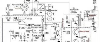
Before moving further, let's look at the circuit diagram of the module. You can download it here - PDF.
There is nothing complicated or magical here. Regular half-bridge: 2 keys at the bottom, 2 at the top, you can solder one at a time. The driver, as written above, is from the 1ED family, very evil and immortal. There is an indication of the power supply everywhere, including +12V at the dc/dc output. The protection is implemented on the AND logic element; if the current exceeds, the comparator will output +3.3V, they will light up the optocoupler and it will pull one of the AND inputs to ground, which means that log.0 will be established and the PWM signal from the drivers will disappear. AND with 3 inputs was used specifically; in the next revision I plan to also add protection against overheating by the radiator and send an error signal there. All sources will be at the end of the article.
Assembling the inverter layout
I thought for a long time about how to demonstrate the operation of the module, so that it would not be too boring, but would be useful, and not too complicated, so that anyone could repeat it.
Therefore, I settled on a voltage inverter, the kind they use to work with solar panels; if something goes off on the low-voltage side, it’s not a big deal, but on the high-voltage side, just don’t put your hands in it when you turn it on. The inverter itself is outrageously simple, by the way, MAP Energy rivets exactly like this, here is an example of even the commercial implementation of this idea. The work of the inverter is to form a sinusoidal alternating voltage with a frequency of 50 Hz from a direct voltage of 12V, because this is what a regular 50 Hz transformer is used to working with. I use some kind of Soviet one, like OSM, the 220V winding is factory-made and is used as a secondary, and the primary ~8V is wound with a copper busbar. It looks like this:
And this monster is only 400 W! The weight of the transformer is about 5-7 kg, it feels like if you drop it on your foot, you definitely won’t be taken into the army. Actually, this is the disadvantage of inverters with “iron” transformers, they are huge and heavy. The advantage of them is that these inverters are very simple, do not require any experience to create and, of course, are cheap.
Now let's connect the modules and the transformer. In fact, the module for the developer should be presented simply as a “black box” that has an input of 2 PWMs and 3 power outputs: VCC, GND and the actual half-bridge output.
Now let's draw our inverter from these “black boxes”:
Yeah, it only took 3 external elements: transformer + LC filter. For the last choke, I made it simply by winding the wire from the module to the transformer on a ring of Kool Mu material, size R32, with a permeability of 60, an inductance of about 10 μH. Of course, the choke would need to be calculated, but we need it in 15 minutes)) In general, if you drive something like that at 400 W, then you need a ring size R46 (this is the outer diameter). Capacity - 1-10 µF film, this is enough. In fact, to save money, you don’t have to install a capacitor, because the capacitance of the transformer winding is healthy... in general, the Chinese and MAP did just that)) The choke looks like this:
All that remains is to throw a test load on the output, I have a pair of 20 W LED light bulbs (I didn’t have anything else visual at hand), they themselves consume 24 W, but the efficiency is the same. Also, the no-load current of the transformer is about 1A. With the battery it will draw about 5A. As a result, we have the following stand:
The prototype also uses a Delta HR12-17 battery, respectively, with 12V and a capacity of 17 Ah. We will control the converter from the STM32F469-Discovery debugging board.
↑ Dual-channel charger
In general, I learned how to discharge batteries, now I need to learn how to charge them.
I know from experience operating a UPS with two batteries that charging batteries in series is not desirable. As a rule, one of the two fails earlier, resulting in a skewed capacity and other special effects. You need a charger to charge two batteries separately, with a limited charge current. I thought for a long time. But I decided to use the FSFA2100 I had already tested for this. Fragment excluded. The full version is available to patrons and full members of the community.
When fully charged, the current in the circuit becomes almost zero, and the battery full charge indicator lights up. At the same time, FSFA2100 can switch to Burst mode, thereby saving energy. I didn’t greatly complicate the system; I don’t see any practical point. A diode is installed in the positive wire of the power supply unit, which allows you to start the power supply unit with the battery connected. Otherwise, the protection allows you to do this only after disconnecting the battery and connecting it again after starting the power supply. An extra diode, but no problem. LED1 and LED2 – power indication, LED3 and LED4 – full charge indication. The threshold for turning on the LEDs 14.2-14.3 V is regulated by selecting R32 and R35.
The ideas used here were collected bit by bit on the Internet, so I do not claim authorship. It is better to select shunts according to the required current; I have 3 of them. 0.47 R each. So far it seems ok.
This is the resulting pothole.
The transformers are wound on cores similar to those I used in the power supply on FSFR/FSFA assemblies. Primary 40 turns Litz 0.07?80. The secondary 5+5 turns is also Litz 0.1×70. The inductance of the primary is slightly underestimated, about 450-470 µH, so there are fewer problems with starting on these trans.
During the work, it turned out that the radiators with the rectifier diodes got very hot, so I had to rack my brains about cooling. How to power the fan? Looking for 24 V? Make a stub? Connect it to only one battery? But then it will be more discharged. Damn, what am I doing? It’s too late to give up... And then I caught my eye on the duty power supply on FSDM0265RN, which I somehow used for experiments with other power supplies.
Fragment excluded. The full version is available to patrons and full members of the community.
A little modification and we got a power supply for powering the fan and relay. Factory transformer. The original output had two voltages - 5 V and 18 V. The winding for 5 V was wound in two wires, so without disassembling the transformer, I separated it and connected it in series. I slightly adjusted the output voltage. It turned out 12 V for the fan and 25 V for powering the relay (I had them at 24 V). Everything is within normal limits.
The purpose of the relay is discussed below, but here is a photo of the device.
This module was made after the charger, so I had to think a little about where and how to attach it.
Here it is on the left facing the main board.
Code
Initially, for control it was supposed to use my STM32VL-Disco, received at the exhibition back in 2010, but it so happened that it was on this layout that it was destined to die after all the code was written and the layout was launched. Forgot about the oscilloscope probes and combined 2 lands, amen. As a result, everything was rewritten on STM32F469NIH6, it was this debugging that was at hand, so there will be 2 projects: for F100 and for F469, both tested. The project was compiled for TrueSTUDIO, version of Eclipse from ST. Code tag
#include “main.h” /**************************************** ***** Sinus table ************************************************** ***************/ uint16_t sinData[240] = {0,13,26,39,52,65,78,91,104,117,130,143,156,169,182,195,207,220,233,246,258,271,284,296,309,321,333,346, 358,370, 382,394,406,418,430,442,453,465,477,488,500,511,522,533,544,555,566,577,587,598,608,619,629,639,649,659,669,678,688, 697, 707,716,725,734,743,751,760,768,777,785,793,801,809,816,824,831,838,845,852,859,866,872,878,884,891,896,902,908,913,918, 923,928,933,938,942,946,951,955,958,962,965,969,972,975,978,980,983,985,987,989,991,993,994,995,996,997,998,999,999,999,999 ,999,999,998,997,996,995,994,993,991,989,987,985,983,980,978,975,972,969,965,962,958,955,951,946,942,938,933,928,923,918,913 ,908,902,896,891,884,878,872,866,859,852,845,838,831,824,816,809,801,793,785,777,768,760,751,743,734,725,716,707, 697,688,678 ,669,659,649,639,629,619,608,598,587,577,566,555,544,533,522,511,500,488,477,465,453,442,430,418,406,394,382 , 370,358,346,333,321,309,296,284,271,258,246,233,220,207,195,182,169,156,143,130,117,104,91,78,65,52,39,26,13,0}; uint16_t sinStep; uint8_t sinStatus; /************************************************ Used functions *** **************************************** ***/ void StartInitClock (void) { RCC->CR |= RCC_CR_HSEON; // Enable HSE while (!(RCC->CR & RCC_CR_HSERDY)); FLASH->ACR |= FLASH_ACR_LATENCY_5WS; RCC->PLLCFGR = 0x00; RCC->PLLCFGR |= RCC_PLLCFGR_PLLM_3; // Div for HSE = 8 RCC->PLLCFGR |= RCC_PLLCFGR_PLLN_4 | RCC_PLLCFGR_PLLN_5 | RCC_PLLCFGR_PLLN_6 | RCC_PLLCFGR_PLLN_7; // PLL mult x240 RCC->PLLCFGR |= RCC_PLLCFGR_PLLSRC; // Source HSE RCC->CR |= RCC_CR_PLLON; while((RCC->CR & RCC_CR_PLLRDY) == 0){} RCC->CFGR &= ~RCC_CFGR_SW; RCC->CFGR |= RCC_CFGR_SW_PLL; // Select source SYSCLK = PLL while((RCC->CFGR & RCC_CFGR_SWS) != RCC_CFGR_SWS_1) {} // Wait till PLL is used RCC->CR |= RCC_CR_PLLSAION; while ((RCC->CR & RCC_CR_PLLSAIRDY) == 0) {} } void EnableOutputMCO (void) { RCC->AHB1ENR |= RCC_AHB1ENR_GPIOAEN; // Enable clock port A GPIOA->MODER &= ~GPIO_MODER_MODER8; GPIOA->MODER |= GPIO_MODER_MODER8_1; // Alternative PP GPIOA->OSPEEDR |= GPIO_OSPEEDER_OSPEEDR8; // Very high speed RCC->CFGR |= RCC_CFGR_MCO1; // Source PLL RCC->CFGR &= ~RCC_CFGR_MCO1PRE; // Div = 1 } void InitIndicatorLED (void) { /* * LED1 - PG6 * LED2 - PD4 * LED3 - PD5 * LED4 - PK3 */ RCC->AHB1ENR |= RCC_AHB1ENR_GPIOGEN; RCC->AHB1ENR |= RCC_AHB1ENR_GPIODEN; RCC->AHB1ENR |= RCC_AHB1ENR_GPIOKEN; GPIOG->MODER &= ~GPIO_MODER_MODER6; GPIOG->MODER |= GPIO_MODER_MODER6_0; // Output PP GPIOD->MODER &= ~GPIO_MODER_MODER4; GPIOD->MODER |= GPIO_MODER_MODER4_0; // Output PP GPIOD->MODER &= ~GPIO_MODER_MODER5; GPIOD->MODER |= GPIO_MODER_MODER5_0; // Output PP GPIOK->MODER &= ~GPIO_MODER_MODER3; GPIOK->MODER |= GPIO_MODER_MODER3_0; // Output PP } void EnableIndicatorLED (void) { GPIOG->BSRR |= GPIO_BSRR_BR_6; GPIOD->BSRR |= GPIO_BSRR_BR_4; GPIOD->BSRR |= GPIO_BSRR_BR_5; GPIOK->BSRR |= GPIO_BSRR_BR_3; } void InitLowPWM (void) { /* * TIM1-CH1 - PA8 * TIM1-CH1N - PB13 */ RCC->APB2ENR |= RCC_APB2ENR_TIM1EN; RCC->AHB1ENR |= RCC_AHB1ENR_GPIOAEN; RCC->AHB1ENR |= RCC_AHB1ENR_GPIOBEN; /*********** GPIO **********/ GPIOA->MODER &= ~GPIO_MODER_MODER8; GPIOA->MODER |= GPIO_MODER_MODER8_1; // Alternative output PP GPIOA->AFR[1] |= GPIO_AFRH_AFRH0_0; // Select TIM1-CH1 GPIOB->MODER &= ~GPIO_MODER_MODER13; GPIOB->MODER |= GPIO_MODER_MODER13_1; // Alternative output PP GPIOB->AFR[1] |= GPIO_AFRH_AFRH5_0; // Select TIM1-CH1N /*********** Timer *********/ TIM1->PSC = 2400-1; // div for clock: F = SYSCLK / TIM1->ARR = 1000; // count to 1000 TIM1->CR1 &= ~TIM_CR1_CKD; // div for dead-time: Tdts = 1/Fosc = 41.6 ns TIM1->CCR1 = 500; // duty cycle 50% TIM1->CCER |= TIM_CCER_CC1E | TIM_CCER_CC1NE; // enable PWM complementary out to PB15 and to PA10 TIM1->CCER &= ~TIM_CCER_CC1NP; // active high level: 0 — high, 1 — low TIM1->CCMR1 &= ~TIM_CCMR1_OC1M; TIM1->CCMR1 |= TIM_CCMR1_OC1M_2 | TIM_CCMR1_OC1M_1; // positiv PWM1_CH3 and PWM1_CH3N TIM1->BDTR &= ~TIM_BDTR_DTG; // clear register TIM1->BDTR |= TIM_BDTR_DTG_2 | TIM_BDTR_DTG_1 | TIM_BDTR_DTG_0; // value dead-time: = 31*Tdts = 32*41.6ns = 1.29us TIM1->BDTR |= TIM_BDTR_MOE | TIM_BDTR_AOE; // enable generation output and dead-time TIM1->CR1 &= ~TIM_CR1_DIR; // count up: 0 - up, 1 - down TIM1->CR1 &= ~TIM_CR1_CMS; // aligned on the front signal: 00 — front; 01, 10, 11 — center TIM1->CR1 |= TIM_CR1_CEN; // start count } void InitSinusPWM (void) { /* * TIM3-CH1 - PB4 * TIM3-CH2 - PC7 */ RCC->APB1ENR |= RCC_APB1ENR_TIM3EN; RCC->AHB1ENR |= RCC_AHB1ENR_GPIOBEN; RCC->AHB1ENR |= RCC_AHB1ENR_GPIOCEN; /*********** GPIO **********/ GPIOB->MODER &= ~GPIO_MODER_MODER4; GPIOB->MODER |= GPIO_MODER_MODER4_1; // Alternative output PP GPIOB->AFR[0] |= GPIO_AFRL_AFRL4_1; // Select TIM3-CH1 GPIOC->MODER &= ~GPIO_MODER_MODER7; GPIOC->MODER |= GPIO_MODER_MODER7_1; // Alternative output PP GPIOC->AFR[0] |= GPIO_AFRL_AFRL7_1; // Select TIM3-CH2 /*********** Timer *********/ TIM3->PSC = 5-1; // div for clock: F = SYSCLK / TIM3->ARR = 1000; // count to 1000 TIM3->CCR1 = 0; // duty cycle 0% TIM3->CCR2 = 0; // duty cycle 0% TIM3->CCER |= TIM_CCER_CC1E; // enable PWM out to PA8 TIM3->CCER &= ~TIM_CCER_CC1P; // active high level: 0 - high, 1 - low TIM3->CCER |= TIM_CCER_CC2E; // enable PWM complementary out to PA9 TIM3->CCER &= ~TIM_CCER_CC1P; // active high level: 0 — high, 1 — low TIM3->CCMR1 &= ~(TIM_CCMR1_OC1M | TIM_CCMR1_OC2M); TIM3->CCMR1 |= TIM_CCMR1_OC1M_2 | TIM_CCMR1_OC1M_1 | TIM_CCMR1_OC2M_2 | TIM_CCMR1_OC2M_1; // positiv PWM1_CH1 and PWM1_CH2 TIM3->CR1 &= ~TIM_CR1_DIR; // count up: 0 - up, 1 - down TIM3->CR1 &= ~TIM_CR1_CMS; // aligned on the front signal: 00 — front; 01, 10, 11 — center TIM3->CR1 |= TIM_CR1_CEN; // start count } void InitStepSinus (void) { RCC->APB1ENR |= RCC_APB1ENR_TIM6EN; // enable clock for basic TIM6 TIM6->PSC = 5-1; // div, frequency 24 kHz TIM6->ARR = 1000; // count to 1000 TIM6->DIER |= TIM_DIER_UIE; // enable interrupt for timer TIM6->CR1 |= TIM_CR1_CEN; // start count NVIC_EnableIRQ(TIM6_DAC_IRQn); // enable interrupt TIM6_DAC_IRQn } /************************************* Main code **** *****************************************/ int main (void) { StartInitClock( ); // EnableOutputMCO(); InitIndicatorLED(); InitLowPWM(); InitSinusPWM(); InitStepSinus(); EnableIndicatorLED(); while(1) { } } /**************************** Interrupts ************ *****************************************/ void TIM6_DAC_IRQHandler (void) { TIM6->SR &= ~TIM_SR_UIF; if (sinStatus == 0) {TIM3->CCR1 = sinData[sinStep];} if (sinStatus == 1) {TIM3->CCR2 = sinData[sinStep];} sinStep++; if (sinStep >= 240) { sinStep = 0; sinStatus = sinStatus ? 0 : 1; } } In general, in my other article, I described in great detail and clearly how to generate a sinusoidal signal, how to write code, and so on. You can read it here.
Have you read it? Want to collect? Keep the project:
- Project for F469
- Project for F100
We run the code, arm ourselves with an oscilloscope and move on. First of all, we check the presence of a signal at the driver input, it should be like this:
It is worth noting that I supply 2 signals drawing a sine to one half-bridge (module), and 2 signals setting 50 Hz to the other. Moreover, one diagonal is “red + yellow”, and the other is “blue + green”. In the article that I gave above it is written about this in detail, in case you didn’t understand. Now that the signals have been sent, we connect +12V and GND from the laboratory power supply to both half-bridges. I don’t immediately recommend using a battery; if you make a mistake somewhere, something might burn out. The protection on the board saves from excess current, but not from obvious mistakes when the plus and minus are mixed up, but the laboratory worker saves. 12V and 1A are enough for tests. We take the oscilloscope probe, its ground wire to the output of the first half-bridge, and the probe itself to the output of the other half-bridge and there should be a picture like this:
Where is the sine you ask? The fact is that the input resistance of the oscilloscope is high and it does not represent a load, so no current flows and there is no place for the sine wave to come from. Let's add a load, I made a 90 Ohm load from 10 Ohm resistors by simply connecting 9 of them in series. We connect the load to the outputs of the half-bridges and see the following picture:
Is it the same with you? So it’s time to connect the choke, transformer, load and try to start it up. Achtung! You cannot turn on this layout without a load, because at idle the output can be up to 350...380V. To avoid this, you need a load or an OS.
We won’t have the latter, this is the topic of a separate article, you can attach a simple P-regulator as an option, you already have a project template.
Inclusion
After switching on, we get about 230V at the output, the output is of course not stabilized and will float 230V + -30V, it will work for tests, in another article we will finalize the layout as I decide to talk about P and PI regulators and their implementation.
Now you can enjoy the result of your work, and if necessary, cram everything into a box and even use it on the farm or in the country to provide yourself with light and other delights.
You probably noticed a delay between the “click”, that is, the supply of power to the Discovery and the turning on of the lamps - this is the time that the MK spent on initialization. This delay can be reduced if you write one digit to the register at a time, rather than splitting the register entry into a bunch of lines. I split it up purely for clarity. Although this is not scary, with HAL code the delay is 3 times longer and people somehow live with it))
Before I forget, the project sources:
- Schematic diagram - PDF
- BOM - Excel
- Gerber-files - RAR
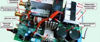
It remains to see how the temperatures on the board are, and whether there are any particularly hot spots. 5-6A is certainly not enough, but if there is a through current or some other serious error, then this is enough to turn the board into a teapot:
As you can see, the hottest element is the dc/dc module for galvanic isolation, which is 2 W, it heats up to 34 degrees, and there’s also a shunt. The transistors themselves and the radiator are at ambient temperature after 30 minutes of converter operation))
The simplest do-it-yourself converter
Self-manufacturing of analog and digital converters is beneficial for the following reasons:
- Low cost. Parts for homemade devices are found in old radio equipment.
- Diversity. There are many options that you can make yourself.
Homemade inverters are built according to a standard design. The device is based on a master oscillator. One or more pairs of transistors are connected to it directly or through a matching transformer. Under the influence of impulses, they begin to switch alternately. The signals enter a step-up transformer and reach a potential of 220 volts.
Necessary materials
In simple converter circuits the following are most often used:
- bipolar transistors – KT 805/819/817/815;
- composite – KT 825/827;
- field - IRF3808/3205, IRL2505, IRFZ40.
They can be replaced with similar characteristics. Most home craftsmen solder parts for them from old amplifiers, tape recorders, printers and other equipment.
Some people use the KR1211EU1 microcircuit to build an inverter. It already has two channels built in for controlling powerful transistor switches.
In accordance with the chosen scheme and design you will need:
- capacitors and resistors;
- transformers and circuits (ready-made or homemade);
- sheets of metal, plastic;
- thick wires (at least 3 mm²);
- fasteners.
Stages of work
Before starting to build the converter, a plan is drawn up. Represent or record the manufacturing steps:
- Search. Find the diagram and details.
- Prepare the tool.
- Installation. Mounted or on a board (you will have to do it yourself or order it).
- Winding a transformer if there is no ready-made one.
- An assembly of sheets of screws or box bolts for the device body.
- Connecting conductors for connecting to batteries and equipment.
Thanks and plans
In the near future, I plan to write about the DSP board and control it not from discovery debugging, but from a “specialized” module.
The 2nd revision boards for it have already arrived from the same PCBway, I’m waiting for the components and writing them right away. I hope you liked the article and the idea itself. In the future, using the same modules, I will show you how to assemble a frequency generator, an mppt controller, and maybe something else interesting. If you have questions, do not hesitate to ask them in the comments or in a personal message, if you suddenly do not have a full-fledged account, I will try to answer all questions.
Now a little thanks to PCBway, it’s actually very good that they support the open source movement. Maybe soon hardware developers will even catch up with software writers in terms of the number and quality of open projects.
↑ Summary
These are the kinds of things that can be triggered by a simple power outage.
This equipment worked on the floor at work for six hours, causing puzzled looks from those passing by. So the system is quite viable. After assembly I remembered one story. Several years ago, a former work colleague of mine received an interesting watch as a gift from the North American states. If you remember, these are the electromechanical Flip Clock watches shown in old films with an indication on flip cards.
So, not only are they 110 V, but the clock itself is synchronized from the mains at 60 Hz (our standard is 50 Hz). Naturally, they were seriously lagging behind in their work and were more like an element of the interior than a watch. Now this problem would be solved very simply. Another possible use for this device has been found.
But there are also three-phase versions! No, that's it, enough experiments for today!