Soon!
Home » Technical information » Articles » The main problems of pure tinOctober 12, 2007
Introduction
The growing attention of modern industry to issues of environmental conservation and concern for public health has recently greatly influenced the composition of the materials and technologies used in the production of electronics. In particular, lead-free soldering technology has become widespread. Lead is a material that causes significant harm to human health, but the refusal to use it in electronics has caused a number of technological problems. Newer lead-free solder alloys are known to have higher melting temperatures, which narrows the process window and thus results in more stringent controllability requirements for the soldering process. Some applications, such as PCB pad coatings and component leads, have begun to use pure tin due to its processability with the transition to lead-free technology. When using pure tin, a number of new problems also arise, primarily related to the properties of this material, which affect the reliability and performance of equipment in harsh conditions. In particular, tin is prone to the formation of filamentous growths - the so-called “tin whiskers” and is susceptible to “disease” in the cold - the so-called “tin plague”.
This article discusses the main problems that can arise when using pure tin instead of lead-containing alloys, their causes, and methods to combat potential defects.
Tin: characteristics and applications
Tin (lat. Stannum) is a chemical element located in the fifth period in group IVA of the periodic system of Mendeleev; atomic number 50, atomic mass 118.69; melting point 231.9°C, boiling point 2620°C, white shiny metal, heavy, soft and ductile. Tin is a rare trace element; tin ranks 47th in terms of abundance in the earth’s crust. It is used primarily as a safe, non-toxic, corrosion-resistant coating in its pure form or in alloys with other metals. The most important alloy of tin is bronze (with copper). Tin, in particular, is actively used to create superconducting wires based on the Nb3Sn compound.
Tin is widely used in the electronics industry as solder and coatings due to its good processability.
Pure tin as coatings
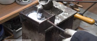
Coating of contact surfaces with pure tin is used to ensure solderability and protect the base metal from corrosion.
With the transition to lead-free technology, many manufacturers began to use pure tin to cover the leads and contact surfaces of components.
Coating of contact pads of printed circuit boards with immersion tin was previously used along with tin-lead coating, due to such a property as surface flatness, which is necessary for making high-quality solder joints. The flat surface of the contact pads coated with immersion tin allows for high-quality surface mounting of multi-lead components, including those with small lead pitches. In addition, the use of pure tin in lead-free technology ensures that there are no impurities of other materials introduced into the solder during soldering. These qualities, combined with a low price, have become a prerequisite for the widespread use of processes for applying immersion tin as a coating.
Immersion tin is chemically deposited onto the copper surface of the printed pattern through a displacement reaction. In this case, the metal of the coated base gives an electron to the tin ion in solution, which transforms into a metallic form, while the base metal dissolves anodicly:
Me0 + Sn2+ -> Me2+ + Sn0.
The standard electrode potential of copper is more positive relative to the potential of tin, so the substitution reaction can only occur in the presence of a complexing agent (thiourea), which shifts the potential to a more negative range of values relative to tin:
2Cu0 + Sn2+ + 4NH2CSNH2 + 2CH3S03H -> 2Cu (NH2CSNH2)2CH3S03 + Sn0 + 2H+[5],
where NH2CSNH2 is thiourea, CH3S03H is methane sulfonic acid [9].
The thickness of the tin immersion coating is about 1 micron.
However, with the beginning of the active use of pure tin with constantly growing requirements for microminiaturization of products, specialists were faced with new manifestations of the features of this material long known in metallurgy: the so-called. "whiskers" of tin and "tin plague".
Tin mustache
The formation of mustaches is a long-known phenomenon. It is characteristic not only of tin; metals such as zinc and cadmium are also prone to the formation of whiskers. In fact, the first published reports of tin whiskers date back to the 40-50s of the 20th century, but little attention was paid to this phenomenon in the electronics industry, since the growth of tin whiskers does not occur in the presence of a lead-containing coating of tin bases, as well as in the presence of a sufficient amount of lead impurity in tin. The use of the classic eutectic tin-lead alloy, which was most widely used before the transition to lead-free technology, ensured the absence of this problem.
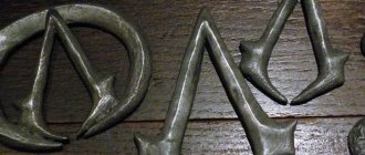
Tin whiskers are thin threads that can grow vertically, bending, spiraling, in the form of hook-shaped or fork-shaped tin crystals. The length of the whiskers can reach 150 microns, which poses a serious risk of shorting adjacent elements of the conductive pattern of the printed circuit board. Whiskers, bending or tearing off during the manufacturing process of products and their operation, can form conductive bridges between current-carrying surfaces. In this case, at a sufficiently high current, the whiskers can melt, causing short-term failures. Whisker pieces can cause both intermittent and permanent product failures.
Rice. 1. An example of bending tin whiskers under a microscope. Photo from [1].
Rice. 2. An example of a tin whisker at 3000x magnification. Photo from [10].
It is impossible to accurately predict the formation of tin whiskers: they can appear both on new products and years after the start of use, both on the elements and under them. They may not appear at all. It is known that whiskers usually grow on coatings with a thickness of over 0.5 μm [9].
Until recently, there was no consensus among experts regarding the reasons for the growth of tin whiskers. Over the past few years, there have been significant advances in the study of whiskers and the main reasons for their formation, but, nevertheless, there is still no final consensus on the causes of this phenomenon. There are also no industry standards defining tin whiskers or regulating methods for combating them.
It has been established that the driving force in the formation of whiskers is the compressive stress in the tin layers. This stress can be a consequence of various reasons, such as the formation of an intermetallic structure, oxidation and corrosion, temperature cycling or mechanical stress [2].
In electroplated tin coatings, tensile stress occurs immediately after deposition, which weakens over time (3-5 days). After 5-7 days, the internal compressive stress begins to increase, which is a consequence of the formation of intermetallic compounds (Cu6Sn5 and Cu3Sn) at the boundary of the tin-copper layers, the molar volume of which is greater in relation to the volume of pure layers of tin and copper. As a result, a helical shear occurs along the grain boundary of the crystal lattice, where the growth of whisker crystals begins [9].
Immersion tin is thin, so no tensile stress occurs after plating. However, whisker growth still occurs, and the reason for their growth is the compressive stress resulting from the growth of the intermetallic layer. Since the thickness of tin is small, its atoms migrate along the boundaries between the metal grains to the place of growth of whisker crystals.
Thin layers of coating are most susceptible to internal stresses, since intermetallic compounds quickly absorb the layer of pure tin completely and oxidize. The optimal thickness of immersion tin, equal to ~1 μm, already poses a serious difficulty for the diffusion of intermetallic compounds [9].
Whiskers or dendrites?
Tin whiskers should not be confused with dendritic growth, which is also a relatively common cause of failure in electronic devices, resulting primarily in intermittent or permanent short circuits. The difference lies not only in the formation process, but also in what is known about the two phenomena.
Dendrites have been well studied because they are not a problem caused by the transition to lead-free technology. They are metal threads or crystals that grow on the surface of the metal (in the x-y plane), and not perpendicular to it (unlike whiskers), in the form of tree-like structures. The mechanism of dendritic growth is electrolytic in nature. That is, for dendrites to grow, it is necessary to have an electrolyte and voltage, and therefore, dendrites can lead to failures only if conditions for the formation of electrolyte are present (for example, humidity plus flux or organic acid residues), and also only during product operation.
Under the influence of the voltage present on the board, the anode conductor dissolves, releasing positively charged metal ions into the channel (Fig. 3a). The ions are directed through the channel to the conductor-cathode, where they are reduced to the metallic state, forming conductive bridges in the form of a dendrite-like loose metal structure in the insulating gap (Fig. 3b) [6]. The growth rate of dendrites at the cathode can reach 0.1 mm per minute [5]. As a result of these processes, whiskers with a thickness of 2...20 μm and a length of up to 12 mm can form in a few minutes (Fig. 3c). After the formation of a thread-like bridge, the crystals gradually thicken to 0.1 mm, acquiring a distinct metallic luster. The resistance of such crystals can reach up to 1 Ohm [6].
Rice. 3. Scheme of dendrite formation in a channel filled with ionogenic contaminants. Figure from [6].
The sequence of dendritic growth is clearly visible in photographs (Fig. 4).
Rice. 4. Stages of growth of metal dendrites: a - 2 min; b - 2.5 minutes; c - 3 min; g - 4 min. Photo from [6].
Dendritic growth is observed on conductors coated with Ag, Cu, SnPb, Au, and AuPd. To avoid the development of dendritic growth, manufacturers control the presence of moisture and chemical residues on the final products, which can dissolve the metal to form ions, which then form dendrites [1].
Intermetallic compounds in tin coating
As is known, Intermetallic compounds or Intermetallic compounds are compounds of two or more metals with each other. Intermetallic compounds refer to metal compounds, or metallides. They are formed as a result of the interaction of components during fusion, condensation from steam, as well as during reactions in the solid state due to mutual diffusion (during chemical-thermal treatment), during the decomposition of a supersaturated solid solution of one metal in another, as a result of intense plastic deformation during mechanical alloying ( mechanical activation) [7]. Essentially, an intermetallic compound is a thin boundary layer of interpenetration of soldered metals into each other.
In solder joints, the intermetallic layer plays the role of a mechanical bond. However, the formation of intermetallic compounds between the tin coating and the base material and their subsequent oxidation are a direct cause of deterioration in solderability. If the thickness of the tin coating is too thin, an ever-growing layer of intermetallic compounds absorbs pure tin, oxidizes and impairs solder wettability [9].
As already noted, the formation of intermetallic compounds may be the cause of the formation of tin whiskers.
The susceptibility of tin to the formation of intermetallic compounds is associated with its structure, which has a body-centered tetragonal crystal lattice. The aspect ratio of the lattice cell (s/a) is less than unity (rectangle in cross section). This non-cubic lattice structure indicates the anisotropic properties of the metal. For tin, the coefficient of thermal expansion and the coefficient of self-diffusion are greater in the direction of the longer side of the crystal cell.
Scientists have noted the unidirectional growth of tin whiskers [9], which is additional confirmation of the connection between the anisotropic structure of tin and the formation of whiskers.
In addition, due to the formation of intermetallic compounds, the appearance of so-called hairline cracks and the formation of weak solder joints is possible, which negatively affects the characteristics of the product.
White Tin "Disease"
The “disease” of white tin depends not so much on the combined use of tin with any other materials, but on its nature.
At the end of the last century, an interesting incident occurred: tin was sent from Holland to Moscow by rail. A train came out loaded with bars of white tin, but it brought only gray powder, useless for anything. On the way, tin “caught a cold” and was “attacked by a plague” [3]. This is one of several legendary stories where economic losses and even deaths occurred due to the tin plague.
Rice. 5. Tin with 5% copper content after prolonged exposure at a temperature of -18°C. Photo from [4].
In reality, this “disease” is the result of a rearrangement of the order of atoms in crystalline tin.
Tin can come in two forms: the first is ordinary silver-white tin, a malleable metal that can also grow in the form of large single crystals. White tin is formed at temperatures exceeding +13.2°C. If the temperature drops below 13°C, then the tin atoms can rearrange and form crystals of another type - brittle non-metallic gray tin. The properties of these two types of tin differ significantly. The density of white tin is 7.3 g/cm3, and that of gray tin is 5.8 g/cm3. The temperature coefficient of volumetric expansion of gray tin is 4 times greater than that of white tin. Internal stresses that arise at the points of contact of different crystal lattices lead to the material cracking and crumbling into powder. The resulting modification already loses the properties of a metal and becomes a semiconductor.
It is known that both white and gray crystals are composed of the same tin atoms. However, the main reason for the difference is the arrangement of atoms in the crystal lattice. Changes in the size and shape of atomic structures completely change the properties of matter [3].
One modification changes to another the sooner the lower the ambient temperature. At a temperature of minus 33°C, the rate of this transformation reaches its maximum. If you pour boiling water over gray tin, then due to strong heating the atoms will rearrange again and the tin will turn back into the white variety.
Among metal physicists, the prevailing opinion is that the transition of white tin to gray begins with “contamination”: gray particles fall on the surface of white tin, and the mechanism of their action is similar to the action of the “seed” during the crystallization of liquids. However, there is an opinion that direct contact between white and gray tin is not necessary for infection with the “tin plague”.
Despite the fact that gray tin is a semiconductor in structure and type of connection between atoms, practically no practical applications for gray tin crystals have yet been found - they are too difficult to grow, they are fragile, and in terms of electrical properties they are no better than germanium and silicon, the industrial production of which fully mastered [3].
Methods to Prevent Tin-Related Defects
Currently, methods have been developed to combat the growth of intermetallic compounds, the appearance of tin whiskers and tin plague, thanks to which the likelihood of their occurrence can be avoided or reduced.
It has been found that various conformal coating materials can help reduce damage caused by tin whiskers. Coatings do not prevent whisker growth, but studies have shown that some coatings slow or inhibit whisker formation. In some cases, the resulting whiskers are “locked” inside the coating, which prevents their development, leading to short circuits [2].
The use of coverings that are not thick or strong enough to control whisker growth is controversial. Coverings that have micro-perforations are generally useless as they allow moisture to penetrate. This moisture creates the conditions for potential dendritic growth and also provides a conduit for whisker formation. Tin whiskers are very stable. They will grow under the covering and, if it is not strong enough, small tendrils may grow through it [1].
In addition, corrosion could theoretically be a significant source of compressive stress in tin films and, as a consequence, could cause whisker growth. Therefore, measures must be taken to prevent severe oxidation and moisture condensation.
The iNEMI Tin Whisker User Group's primary recommendation for whisker suppression is the use of a nickel interlayer between the tin plating and the copper base. Parameters such as thickness, porosity and elasticity of the nickel coating are very important to provide an effective barrier layer for copper [2]. Moreover, due to the creation of such a layer, the diffusion of copper and the formation of tin intermetallic compounds are limited. Plating nickel onto a steel substrate has also been found to be effective.
It is recommended to avoid applying tin over brass as this combination of metals tends to create whiskers. Tin plating of brass can only be used when a nickel diffusion barrier is applied. The minimum thickness of a nickel diffusion barrier is 1.27 µm [2].
If the coating is exposed to prolonged mechanical pressure, the risk of tin whisker growth increases significantly. Careful testing must be carried out to determine whether the growth of whiskers will reduce the reliability of the product.
Tin plague is a fairly rare phenomenon in the electronics industry. Even if coatings of completely pure metal tin are used, after soldering it dissolves in the solder alloy, and in the presence of impurities, tin is no longer susceptible to tin plague. That is why tin is used for soldering and the soldered products do not fall apart. As a rule, absolutely pure tin is not used in coatings of component leads; impurities are necessarily added to it, even a small amount of which can eliminate this problem. If you add a little, for example, bismuth to tin, you can prevent tin plague. Bismuth atoms in the crystal lattice of tin interfere with the restructuring, and white tin remains a metal and does not collapse even at low temperatures. In addition, alloying tin with antimony, cobalt and other metals became a remedy against the tin plague. It was found that aluminum and zinc, on the contrary, contribute to the process of plague formation.
Some manufacturers limit the shelf life of pure tin plated components at lower temperatures. The tin plague effect should also be considered when using solders with high tin content. Since the “tin plague” has a strong effect only at temperatures below -40°C (at near-zero temperatures the transformation process takes many years), its effect on lead-free components is currently poorly studied.
Conclusion
Despite these advances, it is still clear that we do not fully understand the basics of tin whisker formation and the process by which they grow. There are no quantitative models that can predict and forecast whisker growth. The iNEMI Tin Whisker User Group has developed basic methods and standards aimed at reducing the compressive stress in tin films and thereby preventing the formation of whiskers. All of these recommendations are based on empirical data. And if today there are proven methods for preventing the tin plague, it is still impossible to guarantee the complete absence of mustaches after the process of applying tin.
List of sources used
- Advanced coating technologies for lead-free soldiers, Bill Boyd, Specialty Coating Systems, Indianapolis, IN, USA www.globalsmt.net
- iNEMI Updates Tin Whisker Recommendations, Joe Smetana www.globalsmt.net
- About the tin plague and scientific foresight.gornie-porodi.info
- Tin Plague, Andrew D. Kostic, Ph. D. Senior Consultant, Willcor klabs.org
- Technology recommendations about www.spring-e.ru
- Arkady Medvedev. Assembly fluxes. To rinse or not to rinse? “Components and Technologies”, No. 4, 2001 www.compitech.ru
- Intermetallic compounds. www.xumuk.ru
- JSC "OSTEK Enterprise" Encyclopedia of surface mounting. Lead test. Do the components you use contain lead? www.ostec-smt.ru
- Immersion tin as a finishing coating. Reliability comes first! "Technologies in the electronic industry", No. 4, 2007
- Whisker Evaluation of Tin-Plated Logic Component Leads. Douglas W. Romm, Donald C. Abbott, Stu Grenney, and Muhammad Khan. Texas Instruments. Application Report SZZA037A - February 2003.focus.ti.com
all articles
Tin and lead: main differences
Tin is a unique non-ferrous metal that is quite expensive. It is often mixed with other metals in alloys. In particular, it is mixed with lead and this alloy is passed off as pure tin.
In earlier times, these metals were distinguished by color and were called white and black tin. Now you can also tell them apart without even going to a chemical laboratory.
Here are some of the main differences between lead and tin:
- Lead is heavier than tin (about 1.5 times). Even if you don't have a scale handy, you will still notice this difference.
- Color. Pure tin has a silvery and slightly white tint. Lead is darker because it oxidizes in air.
- They have different melting points (232 degrees for tin, 327 for lead).
- The characteristic crunch of pure tin. If you take a rod of tin and start to break it, the metal will begin to crunch. Solder with lead has a softer structure; it can be easily bent, but there will no longer be a characteristic crunch.
But lead is often confused not only with tin, but also with zinc. These 2 metals also have their differences that you need to be aware of.